 Talking Science Podcast
Semiconductors – The Material That Built the Modern World
Pick up a handful of sand on any Australian beach and you are holding the raw ingredient of the digital age. Much of that sand is silica, a compound of silicon and oxygen, and silicon is the second most abundant element in Earth's crust after oxygen itself. Refined to extraordinary purity and patterned with features far too small to see, the same element sits at the heart of your phone, your car, your microwave and the card reader at the supermarket.
What makes silicon so useful is not that it is good at conducting electricity. It is that it is only middling at it, and that its middling ability can be controlled. That in-between quality, the defining trait of a semiconductor, is what the modern world is built on.
Neither One Thing Nor the Other
When it comes to electricity, most materials fall into two familiar camps. Conductors, like copper and most metals, let current flow easily, which is why wires are made of metal. Insulators, like rubber, glass and plastic, block current, which is why wires are wrapped in them. The reasons metals and plastics behave so differently are explored in Why Metals Conduct and Plastics Do Not.
A semiconductor sits between the two. It conducts, but only modestly, and its ability to conduct changes with temperature, light and, crucially, with tiny amounts of added impurities. At first that sounds like a recipe for a useless material. In fact it is exactly what you need to build a switch, because a material whose conductivity you can turn up and down on command is a material you can use to control electricity itself.
The Art of Doping
Pure silicon on its own is not the magic. The magic is a technique called doping, which sounds almost too simple to matter. Doping means deliberately adding minute quantities of another element to pure silicon, sometimes only a few atoms for every million or even billion silicon atoms.
The choice of additive decides what you get. Add an element such as phosphorus, whose atoms bring one more outer electron than silicon's, and you create silicon with a small surplus of free electrons. Because electrons carry negative charge, this is called n-type silicon. Add an element such as boron, whose atoms bring one fewer, and you create gaps where electrons are missing. These gaps, called holes, move through the material and behave like positive charges, so this is p-type silicon.
Neither type is remarkable on its own. The breakthrough comes when you put them side by side.
A One-Way Valve for Electricity
Where n-type silicon meets p-type silicon, a region forms at the boundary, called a p-n junction, and it has a striking property. Current flows across it easily in one direction and hardly at all in the other. It is a one-way valve for electricity, known as a diode.
That simple junction turns up everywhere. LEDs are diodes that release their energy as light. Solar cells are large p-n junctions that do the reverse, turning light into electric current. Australia has a particular claim here: the PERC solar cell design, developed by Martin Green's team at the University of New South Wales in the 1980s, went on to become one of the most widely used solar cell designs in the world.
Arrange doped regions in more elaborate patterns and you get the transistor, invented at Bell Labs in the United States in 1947. A transistor is a tiny switch in which a small voltage on one connection controls whether current flows between two others. String billions of them together and you have a computer. How those switches add up to logic and computing power is the subject of Semiconductors – The Brains of Modern Technology.
The Most Precise Manufacturing on Earth
Instead of wiring transistors together one by one, engineers learned to carve vast numbers of them, together with all their connections, into a single small chip of silicon. Over decades the features shrank relentlessly. A modern processor can contain tens of billions of transistors, with some features measured in mere handfuls of atoms across.
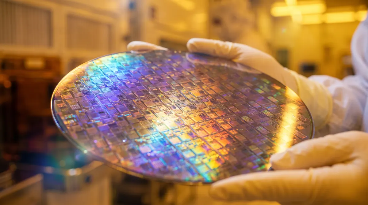
Making them is one of the most demanding things humans do. Silicon is purified to a level where impurities are measured in parts per billion, then grown into large single crystals and sliced into gleaming wafers. Patterns are printed onto those wafers with light, layer upon layer, using some of the most complex and expensive machines ever built. All of this happens in cleanrooms far cleaner than a hospital operating theatre, because a single speck of dust can ruin a chip.
Why Chips Became Geopolitics
That difficulty has consequences far beyond the factory floor. The equipment and know-how for the most advanced chips are concentrated in a small number of companies and countries. When the supply of chips was disrupted during the pandemic years, carmakers around the world had to slow or halt production, and buyers in Australia faced long waits for new vehicles. Governments now treat chipmaking as a matter of national strategy, and restrictions on selling advanced chip-making equipment have become a source of international tension. The whole modern economy runs on these tiny switches, and very few places on Earth can make the best of them.
Running Out of Room
For decades the number of transistors that could fit on a chip roughly doubled every couple of years, a trend known as Moore's Law. That steady shrinking is now much harder to sustain. Features are approaching sizes where quantum effects interfere and there are simply too few atoms left to work with.
Progress has not stopped. Engineers are stacking chips in three dimensions, designing smarter architectures and exploring materials beyond silicon. Researchers at the University of New South Wales led by Michelle Simmons demonstrated a transistor made from a single phosphorus atom placed precisely in silicon, published in 2012, a glimpse of how far the shrinking can go and of the quantum devices that may follow. But the era of easy, automatic doubling is fading, and the path ahead is more varied and less certain. That is not a crisis. It is the normal way a technology matures.
Sand, Made Clever
The semiconductor is the least visible and most consequential material of our age. Purified sand, seasoned with a few carefully chosen foreign atoms, becomes junctions, switches and finally the billions of coordinated transistors inside every device we own. Silicon could not quite make up its mind about conducting electricity, and that indecision, carefully tamed, ended up building the digital world.